
TOKYO, Dec. 5, 2024 /PRNewswire/ — As Moore’s Law almost reaches to its limits, advanced packaging will drive to the next leap in transistor density. The growing demand for AI chips is propelling this evolution of fan-out packaging technologies from wafer-level (FO-WLP) to panel-level (FO-PLP) for more chip integration in devices.
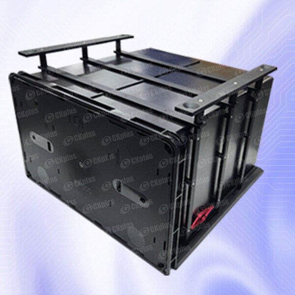
CKplas Panel FOUP 500mm
CKplas has been developing PCB/ABF FOUPs for over 20 years, leveraging decades of experience to seamlessly transition into the Panel FOUP market. Our supported substrates have expanded from wafers to glass. Over half of the world’s top 10 PLP manufacturers are CKplas customers. In addition to Taiwan, our products are now in mass production and supplied to Japan, Korea, the United States, and Europe.
Seizing this market opportunity, CKplas will showcase its latest innovations in SEMICON Japan, held from December 11 to 13 at Tokyo Big Sight, East Hall 1, Booth #1828. We invite customers and industry partners to visit our booth for in depth discussions and to exchange valuable insights on the future of semiconductor technologies.
Media Contact
Lily Lin
TEL:+886-3-3185300
Mail:[email protected]
ข่าวที่เกี่ยวข้อง
- World Young Scientist Summit 2026 Opens in Wenzhou, Zhejiang
- The Results of Phase III OptiTROP-Lung06 Study of Sacituzumab Tirumotecan (sac-TMT) Presented as an ESMO Oral Presentation and Simultaneously Published in The New England Journal of Medicine
- Final OS Analysis Results from Phase III OptiTROP-Lung04 Study of Sacituzumab Tirumotecan (sac-TMT) Presented at 2026 ESMO
- 2026 ESMO | Innovent Announcement Phase 2 Data Presentation for IBI354 (HER2 ADC) In First-line Treatment of Breast Cancer
